Designing for the process: a 3D-printed paperclip and an inverter PCB
Two first-year design projects where the constraint that mattered was the manufacturing process: a printer's resolution, and the rules for laying out a board.
Rayhan M. Project: Nov 2023 Written 3 min read Source on GitHub
These were my first two engineering design projects, from EE194 Project-Based Learning in my first semester at Maynooth. Each ran for about seven weeks in a different team. Neither is technically complex, but both taught the same lesson early: a design that’s correct on screen still has to survive the process that makes it.
The CAD files, board files and reports are on GitHub: 3D-Printed Paperclip and 100 W DC–AC Inverter PCB.
Project 1: A 3D-printed paperclip (Nov 2023)
The brief: a paperclip that holds 10 A4 sheets, can be carried by anyone over 12, and prints in under three hours.
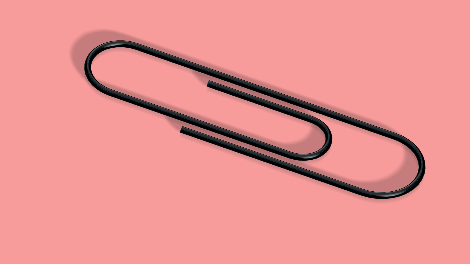
There were seven of us. Instead of agreeing on one idea up front, each of us modelled a different clip in SolidWorks, based on common paperclip shapes, and we printed them all in PLA to test.
Most of the failures had nothing to do with the clip designs themselves:
- Gaps too small to print. A binder-style clip and a thin traditional clip both had gaps narrower than the printer could reproduce. They fused solid, so the clips couldn’t open at all.
- Too stiff. One design held paper well but was too thick to flex comfortably.
- Too loose or too brittle. Others either didn’t grip 10 sheets or felt like they would snap.
The final design was mine. It kept the geometry of a traditional paperclip, with rounded edges so it wouldn’t damage the paper, and tuned the wall thickness and gap spacing to the printer’s limits: thin enough to flex, thick enough to survive printing, with gaps wide enough to stay open. The final two parts printed in 2 hours 50 minutes, inside the three-hour limit.
What I took from it: the CAD model gave no warning about any of the failures. They all came from the printer’s resolution. Printing seven cheap prototypes in parallel found that constraint much faster than more modelling would have.
Project 2: A 100 W DC–AC inverter PCB (Dec 2023)
The brief: design a 100 W inverter that turns DC from a battery or solar panel into mains-style AC, and take it from research through to a manufacturable PCB in EAGLE.
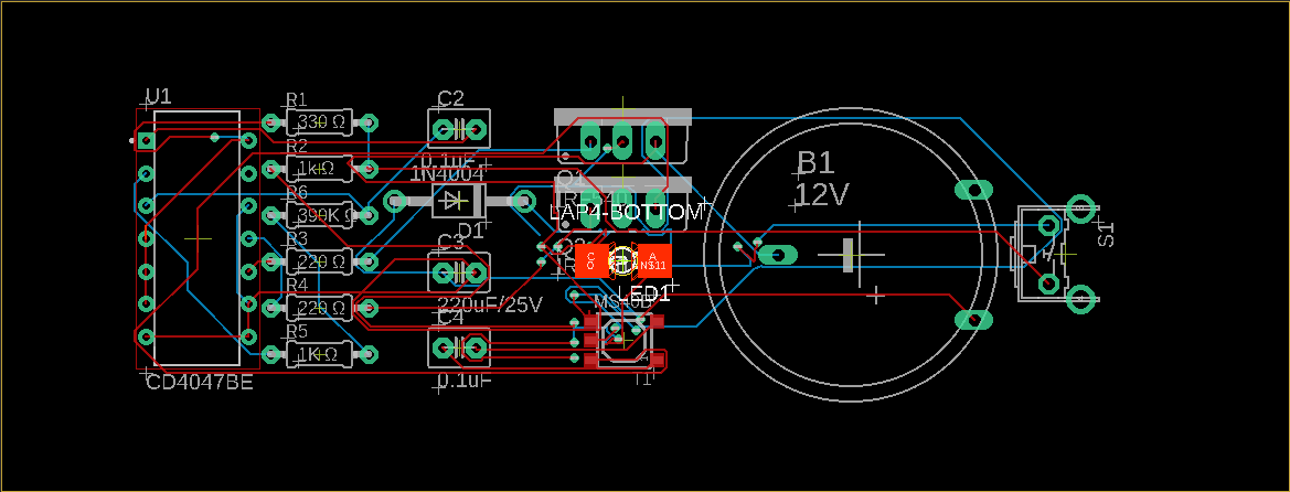
How the circuit works
We chose a common, beginner-friendly design built around a CD4047. The parts list in our EAGLE files shows the core of it:
| Part | Role |
|---|---|
| CD4047 | Astable oscillator: two complementary square-wave outputs |
| 2 × IRF540 | 100 V N-channel MOSFETs, one per output |
| 12 V battery | DC input |
| Large electrolytic capacitor | Smooths the supply |
| 1N4004, LED, switch | Protection, power indicator and on/off |
In astable mode, the CD4047’s Q and Q̄ outputs are opposite square waves at a 50% duty cycle. Each output switches one MOSFET, and the two MOSFETs take turns pulling current through opposite halves of a centre-tapped transformer. Alternating the direction of current in the primary is what produces AC on the secondary, and the transformer’s turns ratio steps 12 V up to mains voltage. The oscillator frequency is set by one resistor and one capacitor (the datasheet gives the period as about 4.4 RC), and is chosen to give 50 Hz.
The output is a square wave, not a sine wave. That’s fine for simple resistive loads, but motors and some electronics don’t handle it well.
From schematic to board
Each of the six of us drew our own schematic in EAGLE, partly so everyone learned the tool and partly to have several candidates. Two were judged strong enough to carry forward, and mine was one of them. I took my design through wiring and board layout to a manufacturing file. The team then compared both boards and picked my teammate’s design as the final one. I also worked on the presentation.
As of the final report the board hadn’t been built or tested, so this was a design exercise, not a working inverter.
What I took from it: a schematic that’s logically correct is only half the job. On the board, trace widths, clearances and heat decide whether it works, and with a mains-voltage output, clearance and isolation become safety requirements rather than tidiness.
- #cad
- #3d-printing
- #pcb-design
- #power-electronics